Wireless Electrophysiology
Introduction
Ever wished you could study brain activity without annoying wires getting in the way? That is the challenge I took on with this project: designing a wireless neural data logging system for recording brain signals in mice. This project aimed to achieve two things: eliminate the need for tethering while maintaining the standard sampling rate (20 kHz) used in these experiments and serve as my introduction to the exciting field of neural engineering—I am currently transitioning from a pure engineering role to a neuroengineering one for my Ph.D.
Design and Fabrication
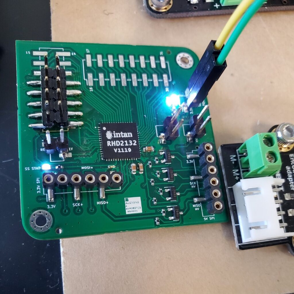
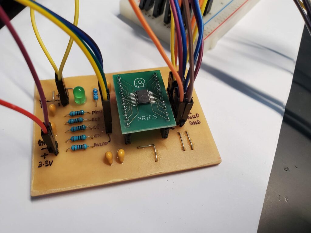
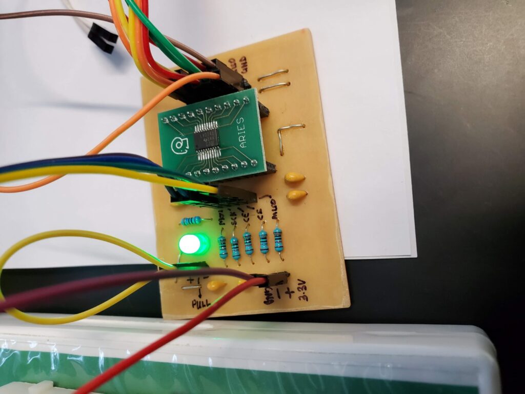
The core of this system lies in the RHD 2132 chip, a powerful 32-channel neural amplifier commonly used in scientific research to capture electrical signals from the brain. To ensure its safe operation, the design incorporates level shifting circuits, protecting the chip from electrical damage. Additionally, the PCB features flexible connection options through pin headers, allowing communication with a microcontroller via either LVDS (high-speed) or CMOS (standard) protocols. Tiny LED lights were also added to help with troubleshooting during the development process.
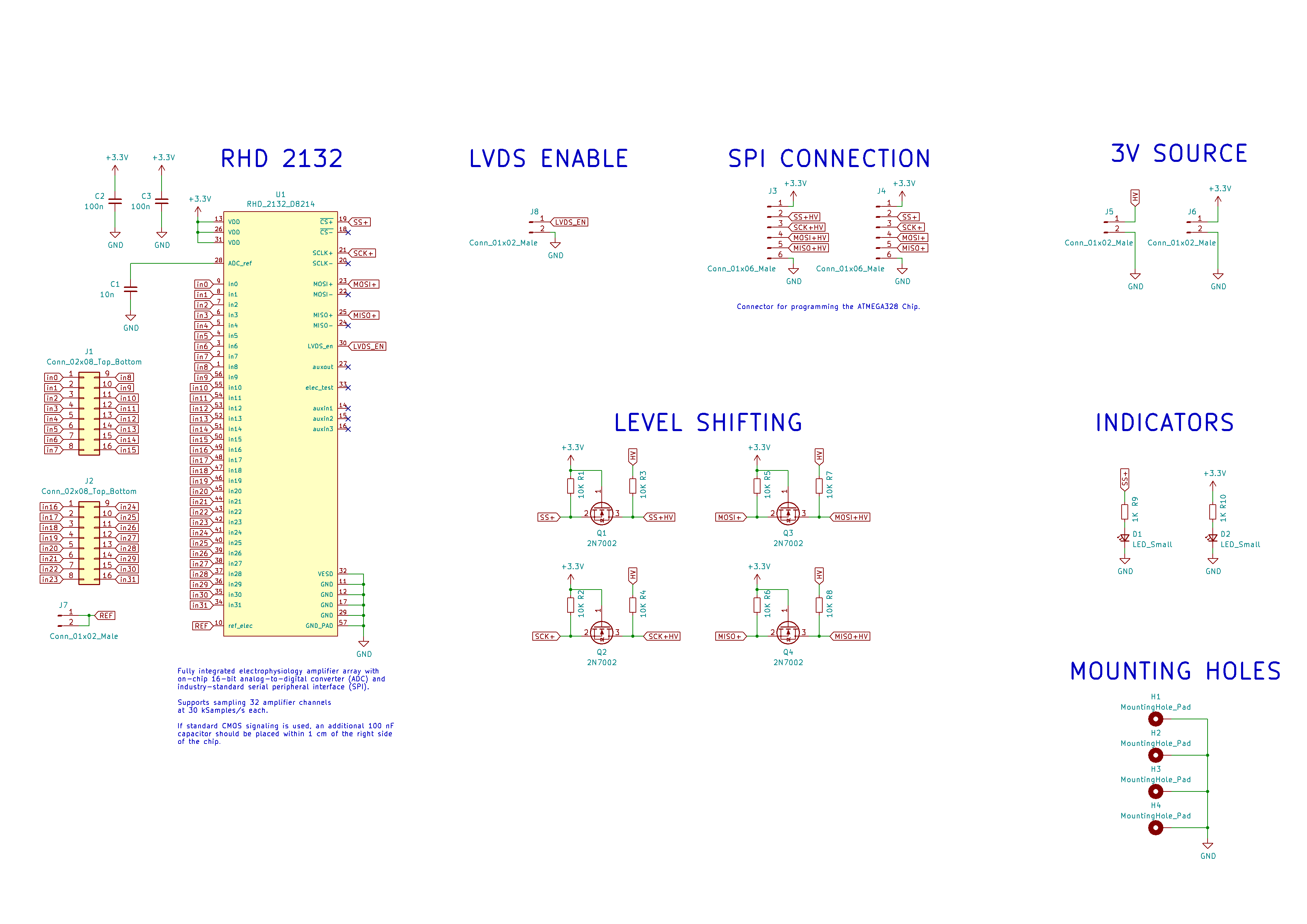
The PCB is made of four thin layers, each with a specific purpose:
- Top and Bottom Layers: These layers carry electrical signals like tiny highways, connecting various parts of the system.
- Ground Plane: This layer acts like a giant electrical sponge, absorbing unwanted electrical noise that could interfere with delicate brain signals.
- Power Plane: This layer delivers the necessary electrical power to run all the components on the board.
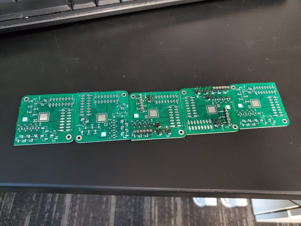

These layers work together to optimize signal quality and minimize noise interference. To further enhance signal integrity, tiny capacitors were placed strategically throughout the board, acting like mini filters to block unwanted electrical noise.
One unexpected challenge arose during the assembly process. The PCB footprint I chose lacked a central hole, making it difficult to hand-solder it securely onto the board. My solution? Carefully drill a small hole to ensure proper placement and electrical contact. The final PCBs were fabricated by PCBWay, a professional service that ensures high-quality manufacturing.
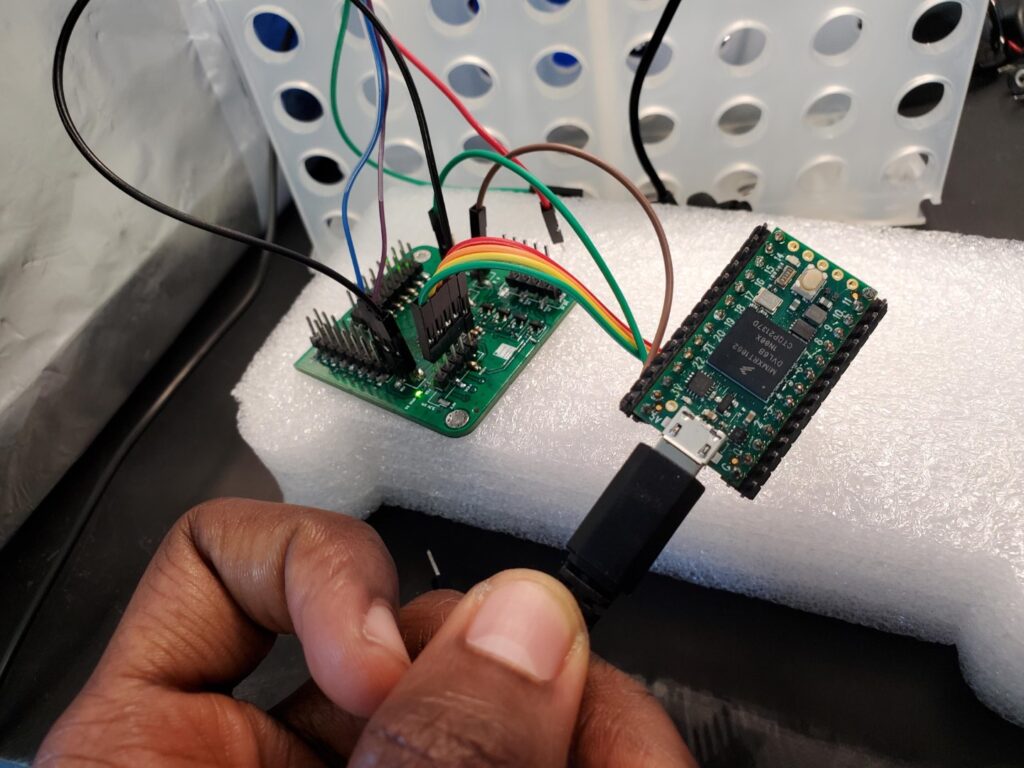
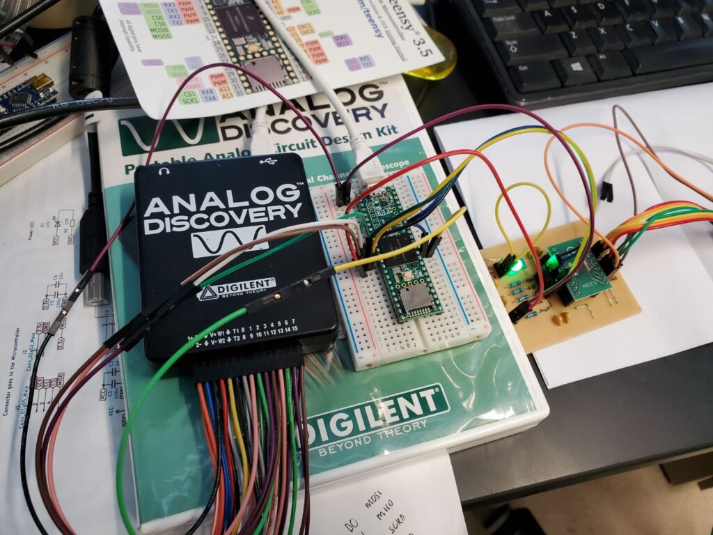
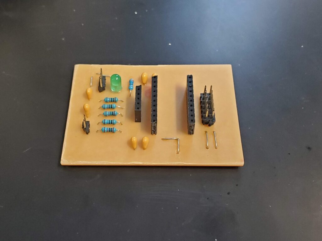
To explore advanced communication options, I designed an additional PCB specifically for Low-Voltage Differential Signaling (LVDS). This technology allows for faster and more reliable data transfer compared to standard methods. This PCB connects a Teensy microcontroller to the main amplifier PCB, enabling efficient communication and data processing. For this additional PCB, I opted for a Bantam OtherMill Pro CNC machine, a powerful tool that allowed for precise milling and fabrication.



Conclusion
Although the project didn’t reach its full potential due to unforeseen circumstances, the journey itself was invaluable. I gained practical experience in various areas, including multi-layer PCB design using KiCad software and understanding the complexities of ephys recording and noise mitigation (I even had to build a miniature Faraday cage to shield the system from external noise!).
This project provided a solid foundation for my future endeavors in neural engineering. The hands-on experience and the challenges I faced equipped me with valuable skills and a deeper appreciation for the complexities involved in this fascinating field.
Skills
- Circuit Design and Prototyping
- Four-layer PCB design
- KiCad
- CNC PCB Fabrication
- Teensy microcontroller
- Ephys recording and noise mitigation
Acknowledgment
Beyond the financial support, I am deeply thankful to the entire Biosensing and Biorobotics Lab for creating a supportive and encouraging environment where I could learn and grow. Their mentorship and guidance throughout this project were truly invaluable.


